Exploring the Capabilities of the SEM Technique: Secondary and Backscattered Electron Imaging
At Anderson Materials Evaluation, our scientific expertise in the SEM technique allows us to provide detailed imaging and analysis of materials at the microscopic level. This page explores the capabilities of secondary electron and backscattered electron imaging, demonstrating how each method offers unique insights into surface morphology and material composition.
Understanding the SEM Technique
The Scanning Electron Microscope (SEM) technique is a powerful tool for analyzing the surface structure and composition of materials. The SEM uses an incident electron beam to produce two primary types of images:
- Secondary Electron Imaging (SEI):
- Resolution: High
- Sensitivity: Surface-sensitive, providing detailed topographical images
- Applications: Ideal for analyzing surface morphology and fine details
- Backscattered Electron Imaging (BEI):
- Resolution: Moderate
- Sensitivity: Atomic mass-sensitive, offering contrast based on element weight
- Applications: Useful for distinguishing different elements and compounds
Illustrative Example: Ni and Ti Wire Specimen
To illustrate the capabilities of the SEM technique, we analyzed a wire specimen consisting of a thick nickel (Ni) wire wrapped with a twisted pair of thinner titanium (Ti) wires.
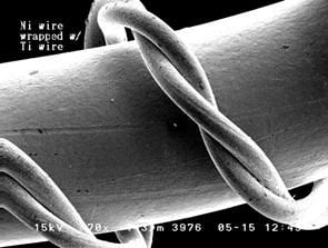
Secondary Electron Imaging (Figure 1)
- Surface Texture: The Ni wire surface shows low rounded bumps, while the Ti wires appear rough and flaky.
- Detail: Excellent resolution, capturing the intricate surface morphology.
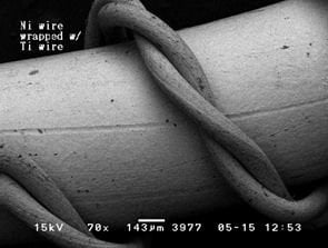
Backscattered Electron Imaging (Figure 2)
- Contrast: The heavier Ni nuclei scatter electrons more effectively, appearing brighter than the lighter Ti and oxygen (O) nuclei.
- Element Differentiation: The contrast difference allows for clear identification of different elements.
Higher Magnification Images
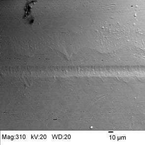
- Ni Wire Surface (Figure 3):
- Magnification: 310x
- Features: Smooth surface with wire drawing lines and elongated pores.
- Debris: Some surface debris is visible.
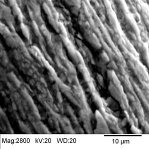
- Ti Wire Surface (Figure 4):
- Magnification: 2800x
- Features: Flaky, scaly appearance with elongated features due to drawing.
- Oxide Layer: A thick oxide layer contributes to the flaky texture.
Combining Imaging Modes for Enhanced Analysis
The combined use of secondary and backscattered electron imaging provides valuable insights that are not typically available through either method alone. This dual approach allows for:
- Comprehensive Surface Analysis: Detailed topographical and compositional information.
- Material Composition Insights: Differentiation between elements based on atomic mass.
- Enhanced Problem Solving: Leveraging scientific expertise for complex materials challenges.
Why Choose Anderson Materials Evaluation for SEM Analysis?
Our team of Ph.D. scientists brings extensive scientific expertise to SEM analysis, ensuring accurate and reliable results for your materials evaluation needs. Whether you require detailed surface imaging or compositional analysis, we have the tools and knowledge to assist you.
Contact Us:
For a consultation on your materials analysis requirements, please reach out to our team. We are eager to explore ways to assist in solving your challenges with our scientific expertise.
