
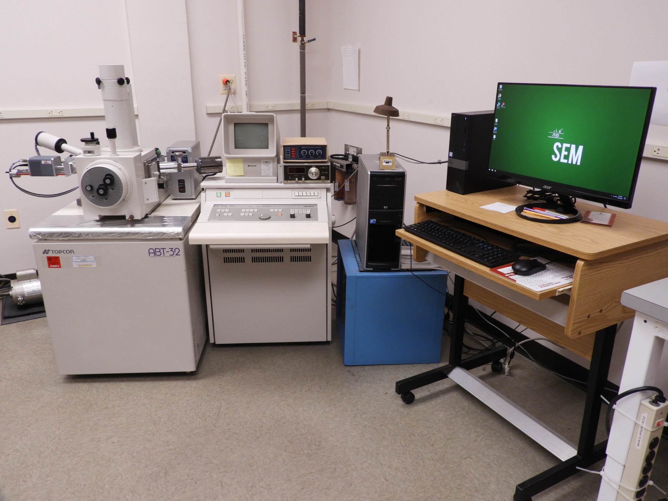
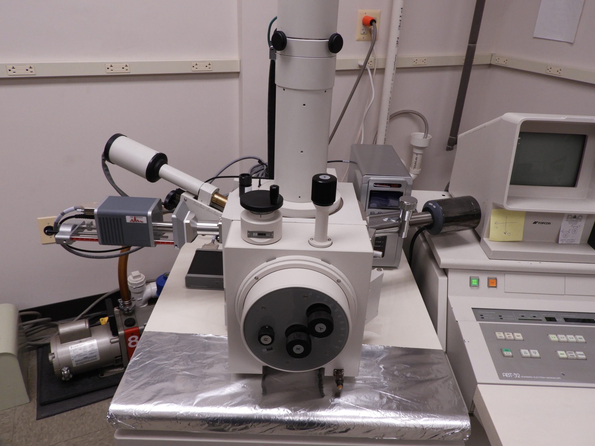
SEM / EDX Capabilities
- Secondary electron images for surface topography, fractography, morphology, crystal structure, particle sizes and shapes
- Robinson electron backscatter detector to distinguish phases and areas based on atomic mass differences with reduced surface sensitivity compared to secondary electron imaging
- Energy Dispersive X-ray (EDX) analysis to measure elemental concentrations to depths of 1 – 2 micrometers and sub-surface diameters of about one micrometer at points or with one and two-dimensional mapping — based on characteristic x-ray emission of elements carbon and heavier in the sample
- Large depth of field to provide well-focused images of rough and textured or fractured surfaces
- Electron beam energies of 2, 5, 10, 15, 20, 25, and 30 KeV to optimally reduce sample charging or damage, to optimize electron beam focus, or x-ray emission for EDX
- High resolution – 5 nm capability, though real materials rarely allow this resolution due to charging issues
- Useful magnifications from 20X – 25,000X
SEM Samples and Materials
- Nearly all engineering materials and solid chemicals, including metals, semiconductors, inorganic particles, glasses, ceramics, many polymers, and some organic particles
- Samples should be carefully prepared for high vacuum compatibility – excessively high outgassing and liquid evaporation is to be avoided, though we have performed SEM of chocolate particles
- The best images are provided by electrically conductive materials because the SEM uses electrons to scan a sample surface
- Many non-metals, ceramics, and organic materials may need to be coated with a conductive material, though low beam energies work with some such materials. We have facilities for coating by sputter deposition. Semiconductors often do not need coating. Where coating will adversely affect the sample properties of interest, low electron beam energies can often be used instead for imaging the sample.
- Cross-section microscopy by SEM sometimes requires coating if sample edges are to be viewed at high resolution when the sample was potted in an epoxy for polishing
- Sample size: from less than 0.1 mm to 150 x 125mm x 50mm height, but samples with the widest dimensions can only be examined near their centers
SEM Applications
- Observe surface topography and morphology at high resolution
- Observe rough or raised-feature surface with great depth-of-field
- Measure thin film and coating thickness with calibration standard reference
- Measure the size of surface features
- Measure particle sizes and determine particle shapes
- Metallographic characterization of metal alloys for precipitated phases, intermetallic phases, and carbides. [See: Metallography]
- Find number and density of surface defects
- Measure number and density of inclusions in metal alloy and determine their kind
- Examine intermetallic phase microstructures
- Determine appearance of stains and residues or deposits on surfaces due to contamination
- Determine whether fracture surface is intergranular or transgranular
- Observe evidence for locus of failure in adhesive bonding failures
- Observe the nucleation sites of the initial chemical attack starting a corrosion problem. Often the key to preventing corrosion is to prevent this initial attack, which may start at a small surface defect, such as an inclusion
- Observe defects in microelectronics dies
- Observe contamination on electronic contacts with enhanced surface imaging at low electron beam voltages
- Examine precipitates at grain boundaries
- Observe damage and defects in micro- and nano-devices
- Observe agglomeration of particles
- Examine quality of surface finish
- Examine microcracking in surfaces, thin films, and coatings
- Find pinholes in coatings
- Examine thin film growth modes, such as columnar growth
- Examine grain size in weld heat-affected zone
- Discover evidence for chemical attack of a surface in very early stages
- Measure the grain size of polished and etched polycrystalline materials
- Examine grain shape and orientation, often important in extruded and rolled materials
- Examine micro-cutting features made by laser cutting techniques
- Examine residues left in sintered ceramics
- Examine pull-out of fibers in composite materials upon fracture for evidence of poor wetting and bonding
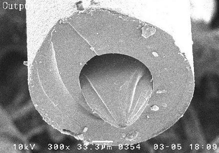
Illustrative Example 1: The broken end of an optical fiber at 300X magnification with SEM/EDX
The crack propagation lines on the quartz core and the surrounding polymer coating can be seen on this insulating and uncoated specimen. The darkened area at the end of the fracture surface on the original glass core surface is very evident. A surface irregularity (most likely a graphitic carbon inclusion at the core surface) caused the concentration of torque and bending stresses resulting in the failure of the fiber. Graphitic carbon microclusters are not uncommon in high purity glass materials exhibiting problems. Such high purity glass is often made by heating a leached glass particle paste with an organic binder to burn off the binder. The burn-off is not always complete, so graphitic or pyrolytic carbon may remain.
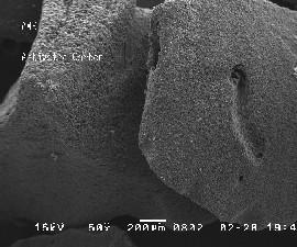
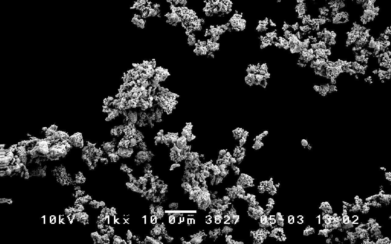
Illustrative Example 2: Activated Carbon
Figure 1 is a low magnification (50X) SEM micrograph of activated carbon particles of an air filter. Activated carbon is similar to graphitic carbon except that it has a high degree of porosity and a large internal surface area. Activated carbon is mostly used as a filter material for removing impurities from water and various gases. Figure 2 is a moderately magnified (1000X) SEM micrograph (of the particle to the right in Figure 1) indicating internal surfaces and porosity in the activated carbon. This sample was sufficiently conductive that it was not coated. The small bright areas on the surface are non-carbon and non-conductive materials.
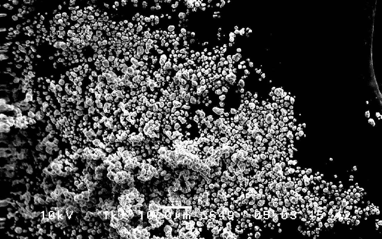
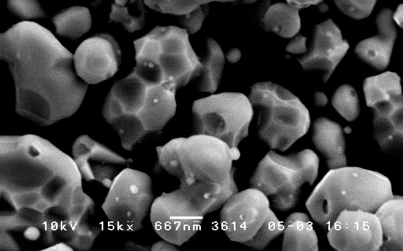
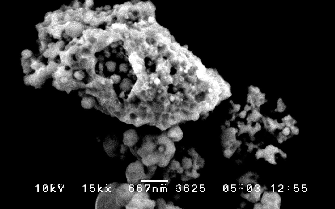
Illustrative Example 3: Evaluation of Powder Particles with SEM/EDX
Particles with nominally the same composition can have very different properties. Figures 1 and 2 show 1 kx and 15 kx magnification images of uncoated particles of transition metal powder “A.” Figures 3 and 4 show 1 kx and 15 kx magnification images of uncoated particles of transition metal powder “B.” The powders are roughly similar in composition but vary in degrees of oxidation. Differences in the tendency of the particles to clump are easily seen at the lower magnifications, while variations in size and morphology become more clear at higher magnification.
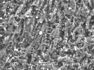
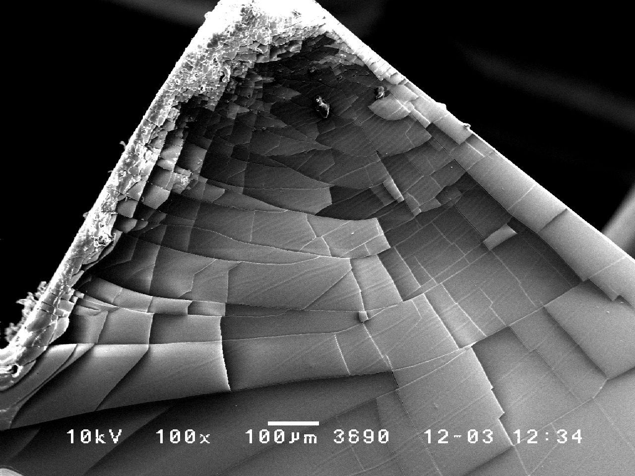
Illustrative Example 4: Sputter Deposited Platinum
A thick layer of sputter deposited Pt on a curved surface shows layering with sharp crystallographic separations, producing an overall “shingled” appearance at relatively low magnification. This is a case in which the great depth of focal field of the SEM compared to optical microscopy is very useful.
| For more on optical microscopy, see: Metallography – Metallographic Microscopy Cross Section Analysis |
| For more SEM Illustrative Examples, see: Comparing Secondary Electron and Backscatter Electron Images for Ni and Ti Wires |
| Top of Page |