
XPS surface analysis provides a quantitative elemental analysis for all elements except hydrogen in the outer 20 nm of a solid surface, as well as much chemical species information. It is used to detect and measure surface contamination, to determine the surface chemistry changes relative to the bulk material chemistry, to examine surface treatments and metal alloy passivation, to examine surface degradation and corrosion, and to examine failure interfaces, such as those of adhesive bond failures. For some materials the surface chemistry is highly differentiated from the bulk chemistry, while for others, it is very similar. We provide highly expert XPS surface analysis services. Please feel free to discuss your surface analysis needs with Charles R. Anderson, Ph.D.
XPS Surface Analysis is also known as: X-ray Photoelectron Spectroscopy or Electron Spectroscopy for Chemical Analysis – ESCA
The XPS Surface Analysis Technique or ESCA
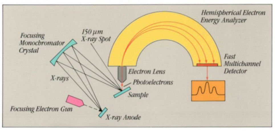
- The sample is irradiated with low energy, monochromatic aluminum anode x-rays, causing the emission of photoelectrons and Auger electrons. Determination of their number and energies in spectral peaks allows the measurement of the number and kind of atoms at the surface. See a longer discussion below.
- High surface sensitivity, commonly with about 50% of the signal from the outer 6 nm of material, about 70% of the signal from the outer 10 nm, and about 90% of the signal from the outer 20 nm
- Quantitative elemental analysis of all elements, except hydrogen and helium, which is generally free of matrix effects which degrade quantitative accuracy, unlike Auger Electron Spectroscopy, EDS, XRF, and FTIR
- Detection limits of 0.001 to 0.005 atomic percent (or 10 – 50 ppm) for heavy metals, 0.03 at.% for lighter transition metals, 0.2-0.4 at.% for O, N, and C, and about 0.4-1.0 at.% for Li, Be, and B
- In weight percent, the detection limit for lead and mercury in most polymers is less than 2 ppm, while that for cadmium is about 3 ppm. Similarly, the weight ppm is also lower than the atomic ppm for these elements in most glasses and ceramics or even most metal alloys.
- Extensive chemical phase identification based on binding energy shifts characteristic of different bonding configurations and quantitative component analysis
- Identification and separation of complex chemical phases by differences in surface potentials using a technique developed by Dr. Anderson in the early 1990s; these complex chemical phases are common on surfaces or interfaces, as they are in minerals
- Depth profiles using ion beam etching for elemental compositions as a function of depth in metals and inorganic materials to depths as great as 3 μm, allowing this surface analysis technique to perform sub-surface analysis
- Elemental composition as a function of depth from 2 μm to 2 mm using a radial sectioner coupled with ion beam etching to clean the final surface of smeared softer materials and the effects of post-abrasion air exposure, allowing this surface analysis technique to perform deep sub-surface analysis
Samples and Materials Suited to XPS Surface Analysis
- Surface analysis of inorganic compounds, ceramics, glasses, polymers, semiconductors, metals, composite materials, and strongly adsorbed liquids or gases on surfaces (such liquid or gas layers are not usually visible)
- Dimensions from sub-millimeter to maximum dimensions of 3″ x 3″ x 0.4″ tall (76mm x 76mm x 10mm), or 5″ x 1″ x 1″ tall (127mm x 25mm x 25mm), or 1″ x 1″ x 1¼” tall (25mm x 25mm x 32 mm), where aspect ratios and weight distributions matter at the maxima. Please discuss your larger sample needs with Dr. Charles Anderson.
- Due to the extremely high surface sensitivity, fingerprints, dust, heavy vapors, cutting oils and fluids, and other contaminants should be kept from contact with surfaces to be studied after those conditions occurred whose effects are to be investigated. Samples to be shipped to us should be in clean containers. The surface to be analyzed should not be allowed to rub against shipping material surfaces.
- In many cases, it is good to send some excess sample real estate so we can select typical area(s) for analysis after microscopic examination and provide microscopic documentation in the report of the areas analyzed
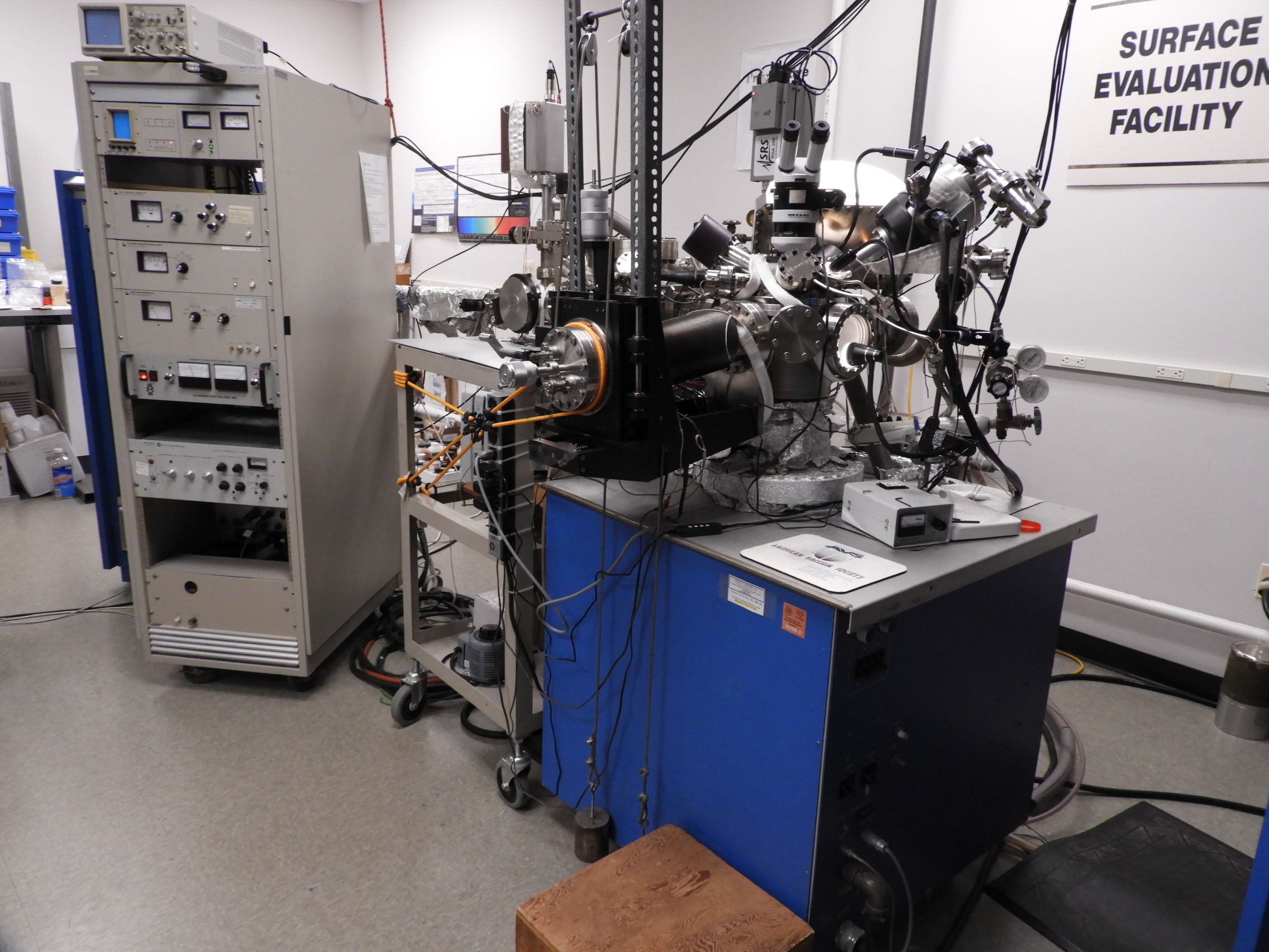
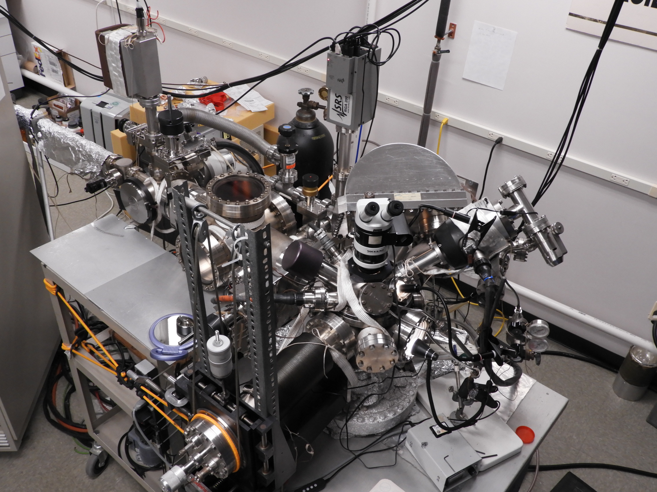
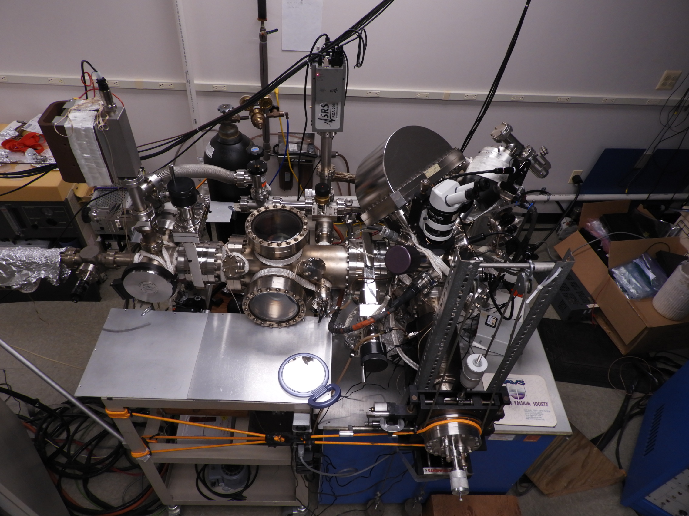
XPS Surface Analysis System Capabilities
- Monochromatic, small-spot low energy (1487 eV) Al x-ray source with 150 – 1000 μm spot sizes, which minimizes radiation damage while providing high energy resolution
- Wide-angle input lens and hemispherical analyzer with simultaneous multi-energy detector for high counting rates
- The UHV system consists of an introduction chamber, buffering sample preparation chamber, and the XPS analysis chamber, with a parallel and linked UHV chamber with an ion pump and mass spectrometer that can open to any combination of the other 3 main chambers. The introduction chamber is pumped with a turbomolecular pump. The sample preparation chamber between the introduction chamber and the XPS analysis chamber has a large ion pump, as does the XPS analysis chamber. Samples pumped in the sample introduction chamber pass through the sample preparation chamber to the analysis chamber, so the analysis chamber is exposed to very little gas load, which is primarily water vapor, when new samples are introduced. The introduction chamber is also brought to atmospheric pressure using nitrogen gas to minimize water absorption on the introduction chamber walls and subsequently minimizing it upon sample insertion.
- Rastered argon ion etching gun to maximize etching uniformity. The ion gun is differentially pumped with a turbomolecular pump to minimize sample contamination due to ion pump regurgitation of active gases caused by hard to pump argon gas.
- Residual gas analyzer (RGA) mass spectrometer with 200 amu range, with both electron multiplier and Faraday cup detection to determine sample outgassing vapors and system background gases
- Sample heating stage for heating to 450°C used with XPS and RGA to examine thermal effects on surface chemistry due to desorption, decomposition, loss of hydration, or reactions
- Angle-resolved sample manipulation for angle-dependent investigations of very near-surface composition variations with depth to provide high depth resolution surface analysis
XPS Surface Analysis Illustrative Examples
- Quantitative Elemental Analysis
- High Resolution Analysis for Chemical Phase Identification
- Depth Profiling to Determine Elemental Composition with Depth
We discuss the issues of whether quantitative elemental composition analysis of a sample is best obtained using EDX, XPS, or XRF or some combination of these complementary techniques elsewhere.
XPS Surface Analysis Application Examples
- Detection and identification of surface contamination
- Failure analysis of adhesive bond failures to identify contamination, component ingredients migrated to the bonding interface, and bonding chemistry
- Highly sensitive and quantitative evaluation of facility silicone contamination using XPS analysis of exposed and returned test kit surfaces
- Identification of causes of corrosion or material degradation including conditions of very early initiation of corrosion
- Surface and near-surface characterizations of process-dependent material compositions
- Detection and identification of optical or abrasion resistant surface coatings and composition analysis to determine chemical stoichiometry
- Soldering, brazing, and welding problem resolution
- Polymer sealing problems
- Cause of intergranular failures in metal alloys
- Stoichiometry of deposited films or chemistry of reacted particle surfaces
- Materials surface composition changes due to chemical leaching, heating, radiation, or absorption
- Identification of unique surface phases of mineral level complexity common in inorganic materials, ceramics, glasses, and metal alloy oxides
- Interdiffusion and reactions at interfaces
- Evaluation of surface cleaning processes
- Medical device and prostheses wear, corrosion, brazing and welding, and contamination investigations
- Surface characterization while heating a material whose components react, outgas, or decompose with additional mass spectroscopy detection of vapor phases
- Semiconductor materials problems for epitaxial materials, bonding pads, barrier and oxide layers, see example of the surface chemistry analysis of an aged silicon oxynitride film
- Nanomaterials surface and interface characterizations
- Metal oxide composition as a function of depth, such as check for chromium enrichment in the surface oxide of stainless steels or to measure the degree of aluminum surface hydration
- Characterize optical coating multilayer structures, such as anti-reflective coatings
- Hard disk drive surface characterization
- Thin film delamination problems
- Environmental cleaning, scrubbing, and adsorbing media characterizations, such as smoke-stack scrubbing lime materials or activated carbon
- Protective coating problems due to mixing problems, segregation of component materials such as plasticizers, slip agents, or fire-retardant chemicals, environmental degradation, fill particle chemistry, and other problems often undertaken with other characterizations such as DSC, TMA, TGA, SEM/EDX, GC-MS, XRF, and optical microscopy
- Identification of fiberglass or other filler fiber and particle materials in plastics, pastes, and composite materials after the burn-off of the polymer matrix, commonly performed by TGA analysis
- Identify cause of adhesive failures at resin/fiber interfaces within fiberglass, carbon fiber, basalt fiber, silicon carbide or nitride or other reinforced composite materials
- Coating analysis, including surface chemistry difference from the bulk coating chemistry
- Chemical characterization of modified and treated surfaces, such as plasma treatments, acid etches and anodizations, and adhesion promoters such as silanes
- Determine bulk chemistry of minerals, ceramics, and glasses by examining freshly ground or fractured surfaces
- Identification of corrosion and wear deposits on hip and knee explants
- Identify the chemistry of gemstones
Direct questions specifically about XPS analysis services to Charles R. Anderson, Ph.D. at canderson@andersonmaterials.com
X-ray Photoelectron Spectroscopy Background and History
XPS surface analysis or ESCA is the result of the Nobel Prize work of two physicists. The first was the explanation of the photoelectric effect by Albert Einstein in 1905, for which he won his first Nobel Prize in Physics in 1921. His work provides the understanding of how a photoelectron is generated. Incoming electromagnetic radiation such as visible light, ultra-violet light, x-rays, and gamma rays incident upon a material surface or an atom in the vapor phase can excite an electron bound to an atom in an electronic orbital into the vacuum. The kinetic energy of this electron is equal to the energy of the exciting radiation minus the binding energy of the electron which was emitted. Since the incoming radiation has no charge and the outgoing electrons do have a negative charge, the material or atom will develop a positive charge, unless it is grounded. Draining this charge results in a photoelectric current, which was the effect that Einstein explained.
In addition to photoelectrons, Auger electrons may also be generated. The nature of the Auger electron emission was described by Pierre Auger, who explained the cause of the Auger electron cascade that follows electron capture by a nucleus in the 1920s. Whatever the cause of an empty core electron hole (an electronic level with a missing electron), an electron from a higher energy level may fall into the empty level and fill that hole. The consequence is that a hole now exists in the higher energy level. This hole may de-excite itself by imparting energy to another electron in an electronic level with similar binding energy. When this happens, this third electron is emitted with a characteristic energy, which is dependent upon the binding energies of all three electronic levels involved in this process. Because of this dependence upon three energy levels, the Auger electron peaks are broader than the photoelectron peaks in a spectrum of electrons emitted from a material when it is irradiated by x-rays.
Kai Siegbahn was the actual inventor of the x-ray photoelectron spectrometer in the 1960s. His father Karl had won a Nobel Prize for work with x-ray spectra in 1924. Kai was in nuclear physics and studying beta-ray emission from decaying nuclei. He was said to be determined to match his father’s success by winning a Nobel prize himself. He built a beta-ray spectrometer and in order to test the spectrometer, he used an x-ray source on materials to generate photoelectrons. These photoelectrons were emitted into a vacuum system and their kinetic energy was measured. The spectrum can be plotted on a binding energy scale by subtracting the kinetic energy measured from the energy of the excitation x-ray, which is usually the low energy aluminum Kα characteristic x-ray at 1487 eV. Kai Siegbahn found that he could not only readily identify the atoms from which the characteristic photoelectrons had come, but that they carried information about the chemistry of the atoms from which they came. For instance, he found that the sulfur 2p photoelectrons had measurably different energies dependent upon whether the material was a sulfide or a sulfate. He found that many other chemical bonds caused sufficient change in the binding energies of the electrons that one could study the chemistry of the emitting atoms in many cases. He also found that the atoms giving rise to the photoelectrons in the sharply-defined peaks were those very near and in the surface of the irradiated material. Even low energy x-rays penetrated the solid materials much more deeply than the thin surface layer from which the photoelectron peaks in the spectrum arose. The great surface sensitivity is due to the use of only those photoelectrons which have not suffered an inelastic collision prior to exiting the material under investigation.
So, Kai Siegbahn had developed a technique to quantitatively investigate the elemental concentrations at material surfaces and to learn a great deal about the chemistry of these surfaces. He named his technique Electron Spectroscopy for Chemical Analysis or ESCA, since there are other means of measuring the elemental concentration, but this spectroscopy is unique in measuring both the elemental and the chemical compositions. Very importantly, it offered a high-powered new surface analysis tool. He won the Nobel Prize in Physics for this work in 1981.
The quantitative analysis of XPS data is primarily dependent upon the probability of excitation of a given electronic level in an atom by the x-ray. A second factor is the mean free path of the emitted electron in a material, which is a measure of the depth from which it is emitted without an inelastic collision. An inelastic collision is a collision involving energy loss of the electron. When the electron loses energy once in such a collision or interaction, it contributes to a feature of the spectrum called a loss peak. These peaks are weaker and broader than the photoelectron peaks and appear in the spectrum as though they are at higher binding energy relative to the photoelectron peak from which they arose. If an emitted electron has two or more inelastic collisions, it contributes to the general background of a spectrum, so the background commonly increases to the high binding energy side of any major photoelectron peak. Because the mean free path lengths are dependent upon the electron energy, increasing as the electron energy increases (in the energy range of XPS), there is a correction for the sampling depth of photoelectrons of different energies. These path lengths for the aluminum characteristic x-ray energy used (1487 eV) are about 1.4 to 2.0 nm commonly. Almost all of the signal comes from the outermost 6-8 nm of material, so the spectroscopy has great surface sensitivity. An example of a wide energy range spectrum can be seen in the Quantitative Elemental Analysis example.
Such techniques as EDS, XRF, and FTIR are often called surface analysis techniques. They should more properly be called near-surface analysis techniques, since they commonly yield signals averaging over depths of 1 to 2 μm. XPS is a truly surface analysis technique with its 8 – 10 nm probing depth being 0.01 to 0.02 times that of EDS, XRF, and FTIR. Because XPS or ESCA uses only those photoelectrons with no inelastic collisions, there is little interaction between the measured signal electrons and the material matrix needing adjustment in quantitative analysis. EDS, XRF, and FTIR all have stronger matrix effects which makes it more difficult to perform accurate quantitative analyses using them.
Further examples of XPS surface analysis of materials:
These examples are often not typical of most of our work, since most of our work is analyses of our customer’s propriety materials, processes, or applications of materials. Some of these application examples are only illustrative of the power of XPS analysis and were actually examinations of common materials not supplied by our customers.
Defective Ceramic Floor Tile Glaze
Detection and Measurement of Silicone Contamination in Facilities and Ovens
Emerald Quantitative Elemental Analysis
Feldspar Multiple Chemical Phase Analysis
Gemstone Coating Claim Investigation
Glass Discoloration and Cracking
Identification of a White Material on Ceramic Floor Tiles
Lead in a Ceramic Dinner Plate – Evaluating the Safety Hazard with XRF and XPS Analysis
Polyethylene Fiber Surface Analysis
Polymer Heat Sealing Investigation
Reflective Coating on Glass Deposition Problem
Silicon Nitride Ceramic Analysis
Silicon Oxynitride Film Surface Chemistry
Silicone Detection on the Surface of an Acrylic Adhesive/Polyimide Tape
Surface Contamination Investigations
Contact: Charles R. Anderson, Ph.D., e-mail: canderson@andersonmaterials.com