Examples of Electronics and Semiconductor Materials Analysis:
For thin material samples, the Ecopia HMS-3000 Hall Effect Measurement System uses the van der Pauw technique for these measurements:
- Measure Electrical Conductivity
- Measure Carrier Concentration
- Measure Mobility
- Measure Average Hall Coefficient
- Measure Sheet Concentration
- Measure Sheet Resistance
- Measure Resistivity
- Measure B-D Cross Hall Coefficient
- Measure A-C Hall Coefficient
- Measure Alpha (Vertical/Horizontal Ratio of Resistance)
- Measure Magnetoresistance
- Depth profile MBE-deposited multi-layer structures on GaAs
- Determine stoichiometry of sputter-deposited or MOCVD materials, such as silicon nitride and titanium nitride films, which are usually really silicon oxynitride or titanium oxynitride films
- Determine cause of soldering, bond pad, and adhesive bond difficulties
- Identify photoresist or wax residues, contaminants, and surface segregated impurities
- Measure thickness and determine uniformity of oxides, nitrides, or other film layers
- Depth profile multifilm contact structures on silicon or GaAs wafers
- Determine composition of thermal compounds or adhesives
- Evaluate the cleanliness of ceramic or plastic packaging materials
- Evaluate PCB laminate interfaces and surface conformal coatings
- Measure contamination on alumina feedthroughs and solve brazing problems
- Determine composition of electroplated gold and other metals, particularly on surfaces to which impurities migrate
- Chemistry of polyimide coating surface and effects on outgassing
- Identity cause of metallization layer delamination
- Detect and identify contaminants on connectors on plastic, ceramic, or pins
- Determine the cause of high contact resistance, such as nickel migration through gold to form NiO on the surface of the gold
- Determine causes of corrosion

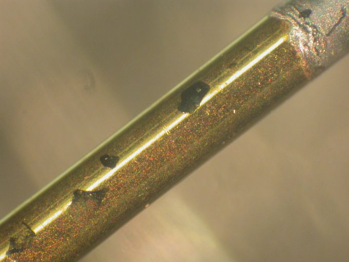
The above pin had a high contact resistance. Black spots on a gold plated pin were analyzed with XPS and found to be NiO. Nickel is commonly plated onto copper wire before electroplated gold is applied over the nickel. If the gold electroplating incorporates too much contamination in the gold layer, easy diffusion paths for nickel to the surface through the low quality gold allow it to seek the oxygen nickel wants much more than gold does.
- Measure the carbon and nitrogen concentrations of organic coatings
- Measure the concentrations of elements heavier than sodium
- Detect very low concentrations of heavy metals down to a few tens of ppm
- Measure the phosphorus and bromine concentrations of fire-retardants in polymer wire insulation and connectors
- Measure the composition and concentrations of inorganic filler materials in plastic connectors and insulation
- Determine the composition of glass in fiber optics
- Measure the composition of fiberglass in circuit boards
- Check the uniformity of fiberglass reinforcement in circuit boards
- Measure the elements inside plastic packaging
- Measure reflectivity as a function of UV and visible light wavelength in coatings and thin films
- Measure the index of refraction of coatings and thin films
- Measure gloss or haze
- Use as a fingerprint for quality control
Infrared Spectroscopy or FTIR analysis:
- Identify flux residue
- Identify wax residue
- Identify thermal compound
- Identify adhesive
- Identify conformal coating
- Identify resin in circuit board
- Identify component plastics
- Identify polyimide coating
- Identify photo resist
- Identify other organic contaminants
GC-MS or Gas Chromatography – Mass Spectroscopy analysis:
- Identify organic components of flux residues, wax residues, thermal compounds, adhesives, conformal coatings, resins in circuit boards, component plastic casings, polyimide coatings, and photo resists which are either volatile or capable of solvent extraction.
- Identify organic materials that may accumulate on electronics from the environment in which they are used.
- Measure thermal expansion properties of materials or IC packages
- Determine softening temperature of plastics & polymers or their degree of crystallinity
- Measure extent and temperature of plastic crystalline transitions
- Measure polymer or plastic glass transition temperature
DSC:
- Measure the specific heat of a material
- Measure energy of intermetallic phase formation
- Measure degree of cure of epoxy materials for electronic packaging or of epoxy adhesives
- Measure melting point temperature of solders, fluxes, waxes, sealants, and potting compounds
- Measure weight loss by outgassing
- Measure degree of water absorption
- Measure total fiberglass content in printed circuit boards
- Evaluate corrosion resistance of coated Kovar hermetic packages
- Strip coated metal layers to measure their thickness
- Measure corrosion rates and pitting potentials of contacts and pins
- Examine corrosion of electronics enclosures
Metallographic / Optical Microscopy / SEM:
- Cross-section analysis of solder joints, connectors, or ceramic capacitors
- Determine polysilicon grain sizes
- Check for voids in PCB material or in solder joints
- Determine whether copper foil layers have the proper surface characteristics in a PCB material
- Examine boards or wafers for anomalies
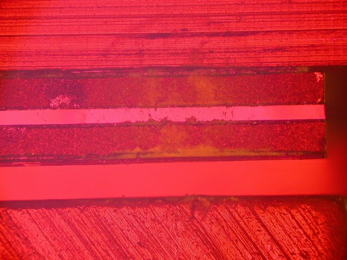
A stain on a laser diode caused by a bad anti-reflective coating on an optical element. The stain and the coating were analyzed with XPS to identify the source of the problem. The image is a Nomarski differential phase interference contrast image.
- Step-height measurements of deposited layers / metallization films
- Surface roughness of metallic films


