
Elemental Composition of Small Volumes of Material
What is LIBS? Capabilities of the Keyence EA-300 LIBS Elemental Micro-Analyzer
- Integrated with the Keyence VHX-7000N Digital Microscope, 4K 3D Optical Microscopy
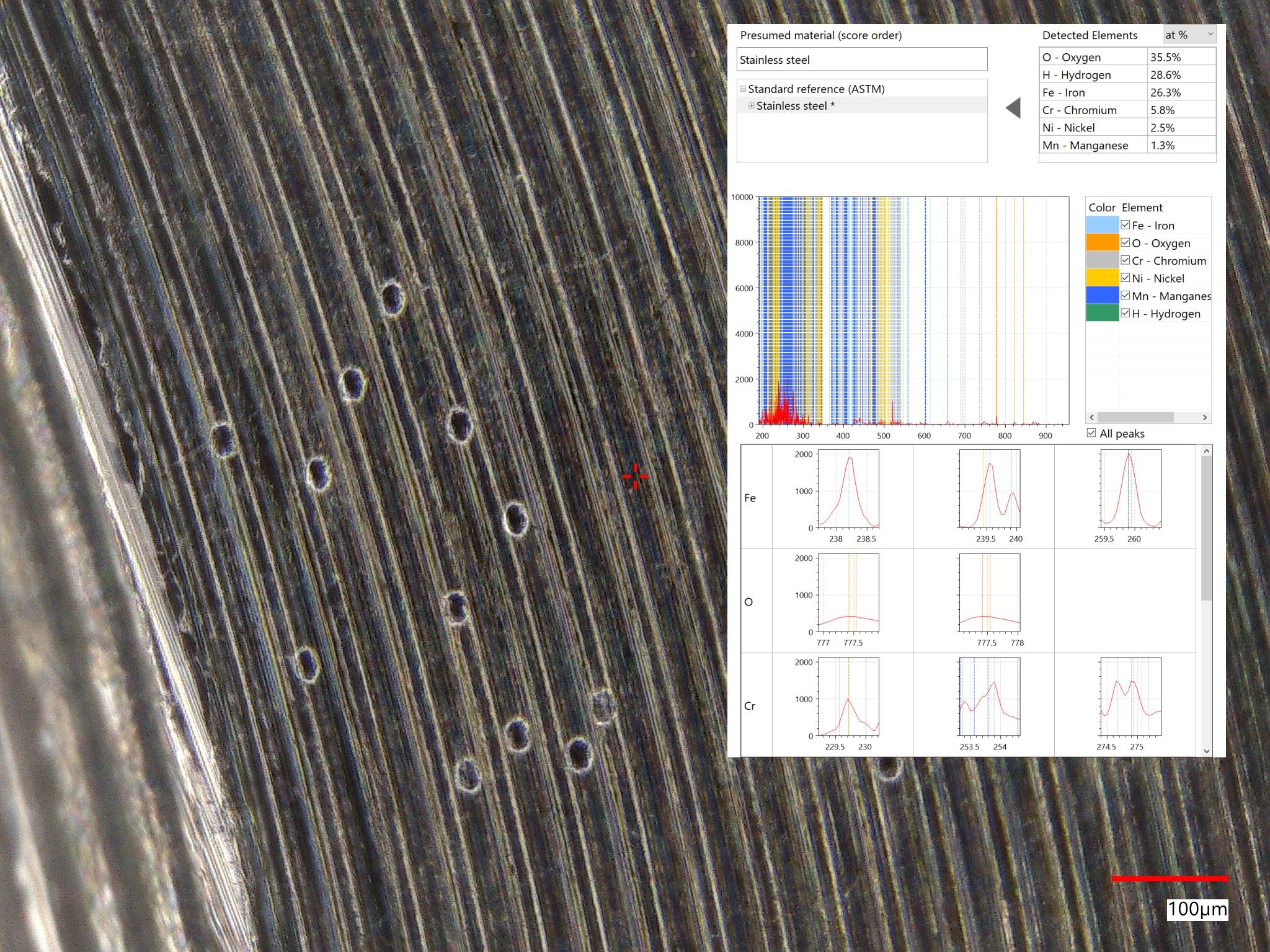
- High power focused 355 nm laser beam ablates a surface area of 10 micrometers diameter with weak, normal, and strong pulse powers
- Crater is usually 5 to 7 micrometers deep — can be deeper and wider for very small objects that may heat up more.
- A plasma results and the de-excitation process emits photons characteristic of the emitting elements in the deep ultraviolet, visible, and near infrared range.
- A 1 by 1.8 inch 3.19 megapixel CMOS sensor detects 185 – 960 nm wavelength radiation through a 300X magnification lens over a 16-bit intensity range for the RGB color of each pixel.
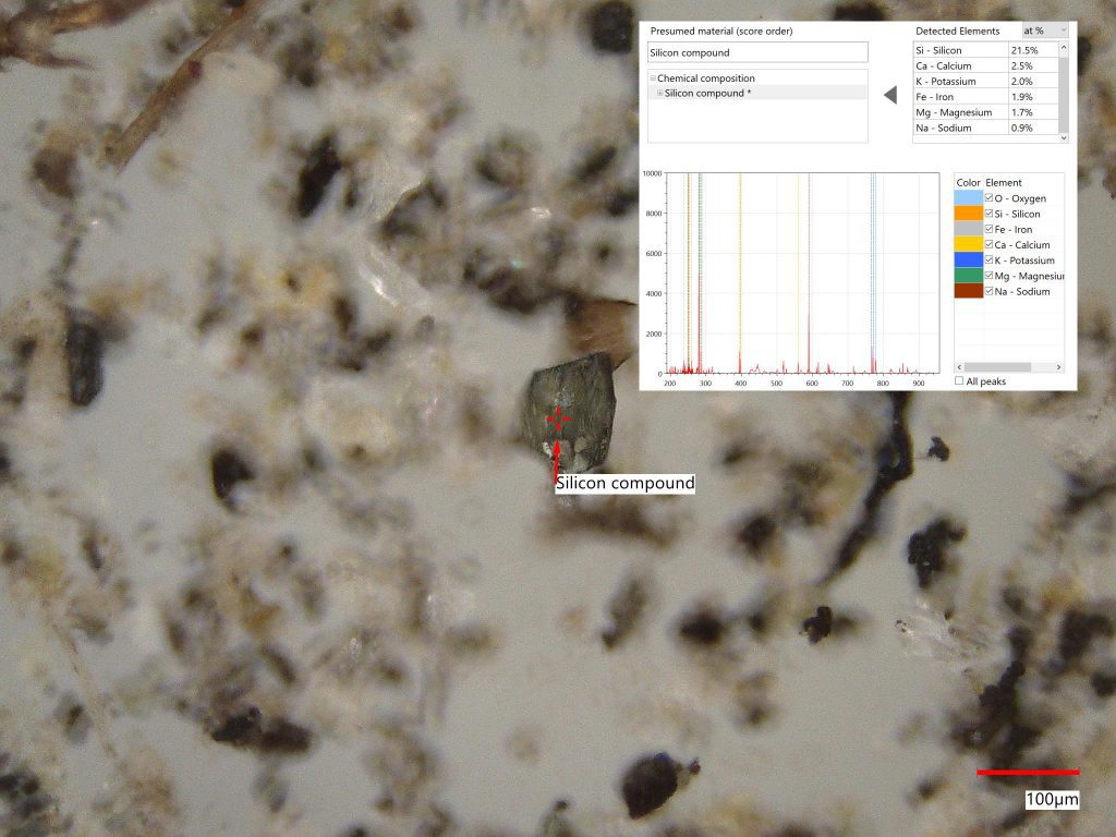
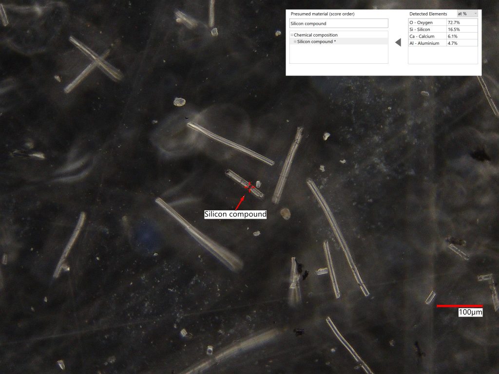
- Identifies and measures elements H, Li, Be, B, C, N, O, F, Na, Mg, Al, Si, P, S, and heavier through U. Does not detect elements well with very electronegative bonding.
- Usually does not detect elements at less than 0.5 atomic percent concentration.
- Single shot mode, drilling mode for depth profiling, and multi-spot analysis mode
- Analyzes about 3 to 4 times deeper into a surface than EDS does with about a 10 times or more wider area. EDS cannot detect or measure the lightest elements.
- Analyzes 300 times deeper than XPS analysis and is much more focused laterally. XPS also detects the lightest elements, except hydrogen.
- Analysis is much shallower than XRF for the heaviest elements and much shallower for the lightest elements. It is much more focused laterally. XRF does not detect many of the lightest elements.
Application Notes
Silicon Nitride Ceramic Analysis
Reach out to us today for your elemental analysis needs, and we’ll gladly engage in a conversation about how our cutting-edge analytical tools can effectively address your concerns.