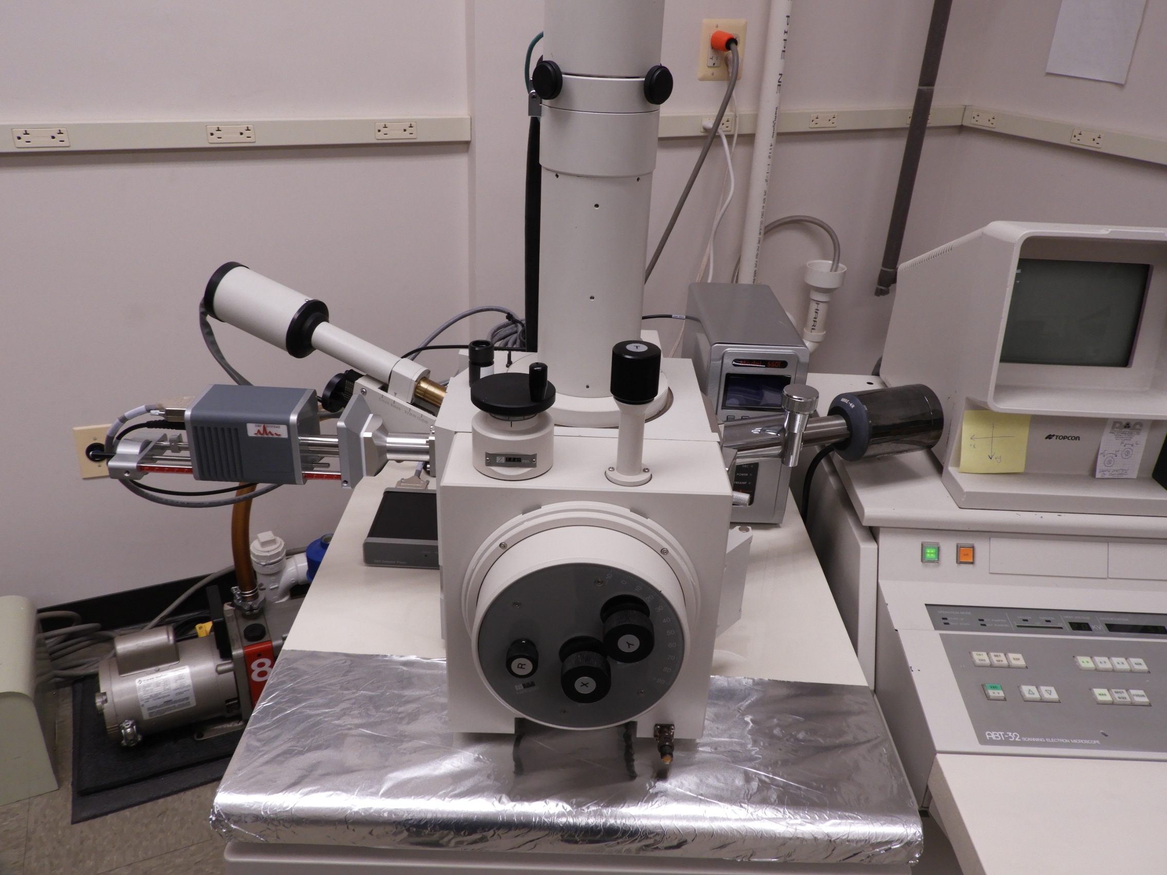
Our EDX / EDS Analysis System and Capabilities
Our Energy Dispersive X-ray (EDX) or Energy Dispersive Spectroscopy (EDS) system consists of a iXRF Systems silicon drift (SDD) light element x-ray detector of 30 mm2 sensor area and 133 eV resolution mounted on our Topcon ABT-32 SEM. The EDX uses the iXRF Systems analyzer and Iridium Ultra microanalysis signal capture, data analysis, and data presentation software. Its capabilities include:
- Acquisition of the full energy spectrum at once during a scan. All detectable elements can be mapped at once, along with either a secondary electron or a backscatter election image.
- Spot, line, and area maps of elements can be generated. These maps may be color coded with several elemental maps superimposed.
- While the secondary electron image may have a resolution of a few nanometers, the x-ray emission spectrum has a much larger volume of material as its source. X-rays are emitted throughout the volume of material into which the electron beam is scattered and decelerated, so the resolution is commonly 1 micrometer laterally and about 1 – 2 micrometers in depth.
- Sample sizes suitable for EDX analysis are the same as those suitable for SEM analysis.
- Quantitative elemental concentrations can be determined at a spot or over an area.
- Image-Pro Plus image analysis software provides counting and sizing and measurement capabilities.
We discuss the issues of whether quantitative elemental composition analysis of a sample is best obtained using EDX or XPS or both techniques elsewhere.
Basic Physics of EDX Analysis
Energy Dispersive X-ray Spectroscopy is based on the detection of characteristic x-rays emitted of an element as a result of the de-excitation of core electron holes created by a high energy electron beam. An electron from a higher binding energy electron level falls into the core hole and an x-ray with the energy of the difference of the electron level binding energies is emitted. Due to the quantization of electron energy levels, the emitted characteristic x-ray energies for elements will generally be different from element to element with only a few spectral peaks overlapping. If the identification of one peak is ambiguous, other peaks or limited knowledge of the sample history will often allow a reasonable elemental identification of the peak.
The normal electron beam of a scanning electron microscope is used as the excitation source. The sample is effectively the anode of an x-ray source. The addition of an energy measuring x-ray detector with a thin, low mass element window on a SEM enables EDS for all elements from carbon on up in atomic mass. A spectrum consists of all of the characteristic x-rays emitted by the elements present in the sample on a continuous background due to Bremsstrahlung x-ray emission caused by the deceleration of the high energy electrons of the electron beam in the sample.
Illustrative Example:
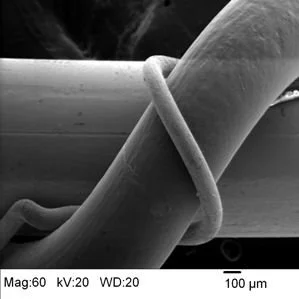
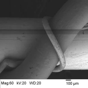
The three-wire specimen shown below was created to illustrate specific capabilities of the combined SEM/EDX system. These include SEM imaging by secondary electrons and backscattered electrons in combination with compositional analysis and elemental mapping using EDX (also sometimes called EDS). When orbital electrons are ejected from an atom as a result of an interaction involving the incident electron beam higher level electrons drop in to fill the resulting “hole” with a concurrent release of a specific amount of energy in the form of an x-ray. These characteristic x-rays as well as the continuum x-rays that make up the background signal emerge from a significantly greater volume of material than the secondary or backscattered electrons. This volume may extend as deep as 1 mm below the surface; an important point to bear in mind when examining features that are on the order of 1 mm or less in dimension.
To create the current example specimen the thinnest wire was wound around the medium diameter wire, and that set was wound around the greatest diameter wire. The specimen is shown in SEM secondary electron and backscattered electron image modes in Figure 1. The secondary electron image (left) shows more of the surface morphology particularly for the medium diameter wire. The backscattered electron image (right) shows different contrast levels for the three wires, but care must be taken to distinguish contrast due to position with contrast due to composition. Directing attention to the lower right quadrant of this image we see that the largest diameter wire appears brightest and is there for probably composed of the heaviest element(s) represented in this sample, followed by the thinnest diameter wire, and finally the medium diameter wire. Also note that at the lowest curve of the thinnest wire there is a contrast change suggesting that there is a layer of foreign material on the thin wire at that location. There is no clear indication of this in the secondary electron image at this low magnification.


The EDX technique can be used to determine the composition of a specimen as a whole as well as the composition of individual components. X-rays that have sufficient energy to escape the material surface can be detected, resulting in a spectrum with peaks at the characteristic energies for the elements present. Elements as light as C can be detected in this way. The areas under selected peaks can also be used to provide semi-quantitative elemental composition information. As an example, consider Figure 2. The inset shows an inspection field within which EDX data were collected by rastering the incident electron beam to produce the spectrum shown. The tabulated results provide a semi-quantitative view of the elemental composition in the inspection field in units of both weight percent and atomic percent. The results reveal that Al, Ti, and Ni are the main elements present within the inspection field, with Al being the most abundant. Given the selected inspection field this suggests that the medium diameter wire is composed of Al. A method to confirm this is discussed next.
Instead of rastering over a relatively large inspection field single points may also be defined and analyzed. In Figure 4, the inset shows the same image again but now with three unique points identified; one on each wire. The resulting spectra show that each wire represents one of the metals detected in the inspection field; the thickest diameter wire is composed of Ni, the medium diameter wire of Al as expected, and the thinnest of Ti. This agrees well with the backscatter image contrast results. Also note that there is slight Al contamination on the other wires based on the EDX spectra. This probably occurred when winding the wires together to form the specimen as Al is extremely soft.


Another important and useful capability of the EDX technique is x-ray mapping of elements. Here the positions of specific elements emitting characteristic x-rays within an inspection field can be indicated by unique color. In Figure 5 the maps of Ni, Al, and Ti are shown individually and overlaid with the original image. Note that the color-coded elements align with the individual wires. While in this example specific elements are associated with specific wires, in more complex samples elemental mapping can be used to great advantage to show positions of inclusions, phases with varying composition, contaminants, etc.


Please contact us about your analysis needs and we will be happy discuss how we can assist you.
